Chip stacking
– HW Choi
Publication Date: 2012
Patent Office: US
Patent Number: US Patent Application 2012/0292788
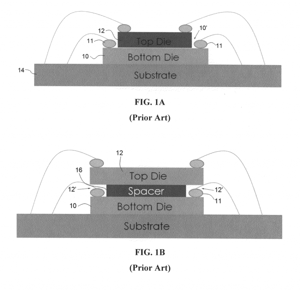
Methods and systems are provided to utilize and manufacture a stacked chip assembly. Microelectronic or optoelectronic chips of any dimensions are directly stacked onto each other. The chips can be of substantially identical sizes. To enable forming the stacked chip assembly, trenches are laser micro-machined onto the bottom surface of a chip to accommodate the bond wedge/ball and wire path of the chip beneath it. Consequently, chips can be tightly integrated without a gap and without having to reserve space for the bond wedges/balls.


 with monolithically-integrated photodetectors for in situ real-time intensity monitoring")


