Close-packed hemiellipsoid arrays: A photonic band gap structure patterned by nanosphere lithography
– WY Fu, KKY Wong, and HW Choi
Applied Physics Letters, vol. 95, 13, pp. 133125 (2009)
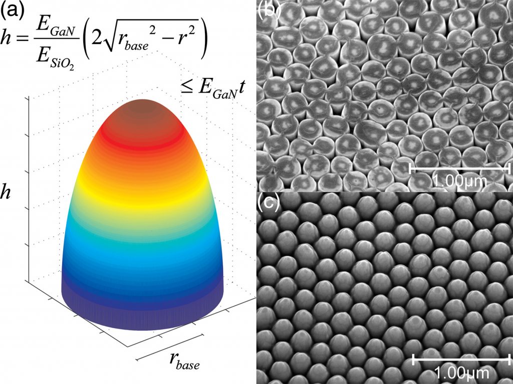
A self-assembled hexagonal close-packed hemiellipsoidal photonic crystal structure was fabricated on GaN material. An ordered monolayer silica nanosphere coating served as a hard mask in an inductively coupled plasma etching process. The shape of the arrayed hemiellipsoids can be controlled by adjusting the etch selectivities and durations according to the fabrication model. The existence of a photonic band gap is established through planar transmissivity measurement whereby a transmission dip centered at 440 nm was identified. A threefold enhancement in light extraction was achieved, as determined from the measured angular photoluminescence emission pattern.
DOI: 10.1063/1.3238564


