GaN PNP light-emitting bipolar junction transistor
– WY Fu, and HW Choi
Journal of Physics D: Applied Physics, vol. 55, 1, pp. 015101 (2021)
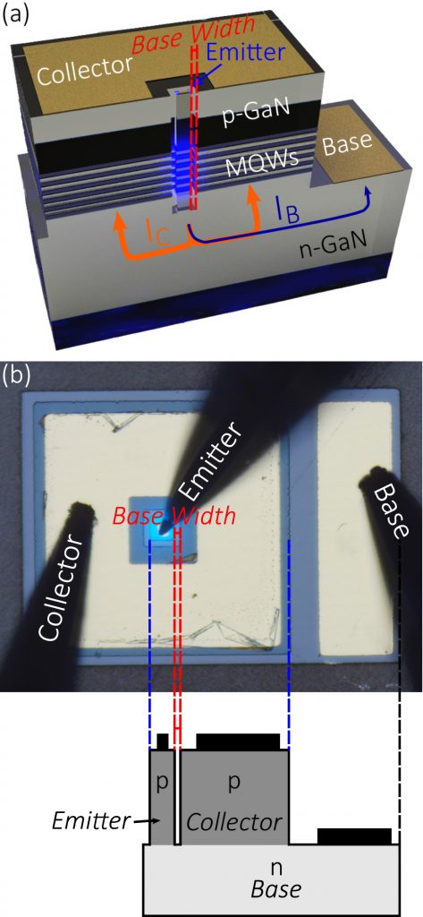
An light-emitting bipolar transistor (LEBJT) has been developed in response to aspirations for on-chip electronics with GaN-based light-emitting diode (LED) devices. The design utilizes the existing p-n junction of an LED structure to construct a PNP bipolar junction transistor comprising two back-to-back p-n junctions, saving the need for customized structures or epitaxial regrowth. Two designs of monolithic GaN LEBJTs have been demonstrated in this work—an LEBJT with a larger emitter area size for conversion of electronic to optical signal, as well as an LEBJT with reduced emitter area for boosting of current gain. Employing an emitter comprising an array of nanopillars patterned by nanosphere lithography, the LEBJT exhibits an average current gain of 20 and a bandwidth of 180 MHz.


