InGaN light-emitting diodes with indium-tin-oxide photonic crystal current-spreading layer
– KH Li, and HW Choi
Journal of Applied Physics, vol. 110, 5, pp. 053104 (2011)
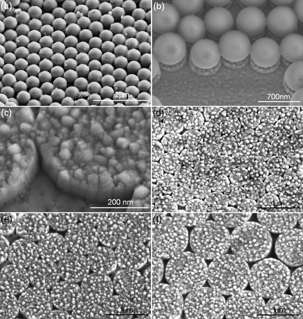
Photonic crystal patterns on the indium tin oxide layer of an InGaN/GaN light-emitting diode are fabricated via nanosphere lithography in combination with dry etching. The silica spheres acting as an etch mask are self-assembled into a hexagonal closed-packed monolayer array. After etching, the photonic crystal (PhC) pattern is formed across the indium-tin-oxide (ITO) films so that the semiconductor layers are left intact and thus free of etch damages. Despite slight degradation to the electrical properties, the ITO-PhC light-emitting diodes (LEDs) exhibit enhancements of their optical emission power by as much as 64% over an as-grown LED. The optical performances and mechanisms of the photonic crystal LEDs are investigated with the aid of rigorous coupled wave analysis and finite-difference time-domain simulations.
DOI: 10.1063/1.3631797


