InGaN nano-ring structures for high-efficiency light emitting diodes
– HW Choi, CW Jeon, C Liu, IM Watson, MD Dawson, PR Edwards, RW Martin, S Tripathy, and SJ Chua
Journal of Crystal Growth, vol. 268, 3-4, pp. 527-530 (2004)
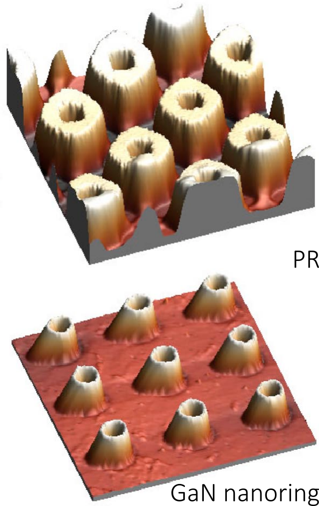
A novel method of etching which allows the direct interconnection of multiple GaN-based devices is introduced. The mesa structures of devices are etched using an isotropic recipe which produces tapered sidewalls. The extent of inclination can be readily controlled through variA technique based on the Fresnel diffraction effect for the fabrication of nano-scale site-controlled ring structures in InGaN/GaN multi-quantum well structures has been demonstrated. The ring structures have an internal diameter of 500 nm and a wall width of 300 nm. A 1cm−1 Raman shift has been measured, signifying substantial strain relaxation from the fabricated structure. The 9 nm blueshift observed in the cathodoluminescence spectra can be attributed to band filling and/or screening of the piezoelectric field. A light emitting diode based on this geometry has been demonstrated.
DOI: 10.1063/1.1849439


