Monolithic Broadband InGaN Light-Emitting Diode
– C Feng, J-A Huang, and HW Choi
ACS Photonics, vol. 3, 7, pp. 1294-1300 (2016)
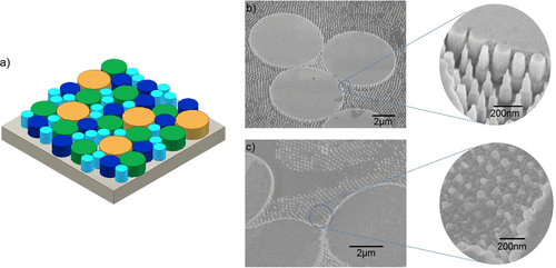
A monolithic nonphosphor broadband-emission light-emitting diode is demonstrated, comprising a combination of high-density microstructured and nanostructured InGaN-GaN quantum wells fabricated using a top-down approach. Broadband emission is achieved by taking advantage of low-dimensional-induced strain-relaxation of highly strained quantum wells, combining light emitted from strain-relaxed nanotips at wavelengths shorter than the as-grown by as much as 80 nm with longer-wavelength light emitted from the larger nonrelaxed microdisks. The localized emission characteristics have been studied by spatially resolved near-field photoluminescence spectroscopy which enabled both the photoluminescence intensity and spectrum from individual nanotips to be distinguished from emission at the larger-dimensioned regions. Distinctive blue-green-yellow emission can be observed from the electroluminescent device, whose continuous broadband spectrum is characterized by CIE coordinates of (0.39, 0.47) and color rendering index of 41. Emission can be tuned by adjusting the relative densities of nanotips and microdisks along the linear color gamut defined by their respective CIE coordinates.
DOI: 10.1021/acsphotonics.6b00269


