Monolithic Integration of GaN-on-Sapphire Light-Emitting Diodes, Photodetectors, and Waveguides
– KH Li, YF Cheung, WY Fu, KK Wong, and HW Choihoi
IEEE Journal of Selected Topics in Quantum Electronics, vol. 24, 6, pp. 1-6 (2018)
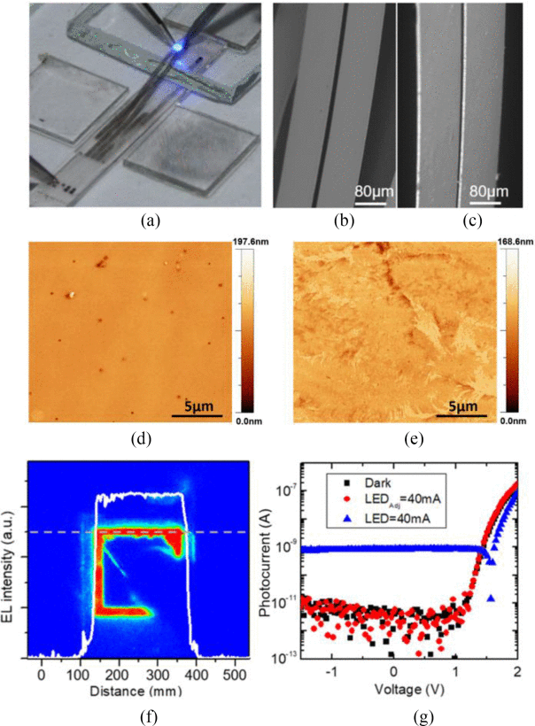
We demonstrate the monolithic integration of light-emitting diodes (LEDs), photodetectors (PDs), and waveguides on a GaN-on-sapphire wafer. The InGaN/GaN multi-quantum wells (MQWs) play a key role in light emission from the LED and photodetection from the PD. Despite large Stokes shift between absorption and emission energies in the InGaN layer, the MQWs are capable of absorbing light emitted by the LED due to the band tail effect, extending the absorption range up to 460 nm. The existence of optical crosstalk is mainly due to optical channeling in the transparent sapphire substrate beneath the LED, but can be eliminated by the detachment of the LED and waveguide via selective-area laser lift-off process. With the bendable waveguides and remounting of the LED onto an elevated platform, the feasibility of routing optical signal between two different planes is demonstrated. Apart from crosstalk-free performance, the three-dimensional system exhibits more than five times higher photocurrent than the planar system, attributed to spectral blue-shift of the LED and enhanced optical confinement in suspended waveguide. The LEDs and PDs also exhibit rapid response on the nanosecond time-scale, enabling transmission of data signals at rates of 250 Mb/s with an opening in the eye diagram.


