Confocal microscopic analysis of optical crosstalk in GaN micro-pixel light-emitting diodes
– KH Li, YF Cheung, WS Cheung, and HW Choi

Applied Physics Letters, vol. 107, 17, pp. 171103 (2015)
The optical crosstalk phenomenon in GaN micro-pixel light-emitting diodes (LED) has been investigated by confocal microscopy. Depth-resolved confocal emission images indicate light channeling along the GaN and sapphire layers as the source of crosstalk. Thin-film micro-pixel devices are proposed, whereby the light-trapping sapphire layers are removed by laser lift-off. Optical crosstalk is significantly reduced but not eliminated due to the remaining GaN layer. Another design involving micro-pixels which are completely isolated is further proposed; such devices exhibited low-noise and enhanced optical performances, which are important attributes for high-density micro-pixel LED applications including micro-displays and multi-channel optical communications.
DOI: 10.1063/1.4934840
Pixel-to-pixel fiber-coupled emissive micro-light-emitting diode arrays
– L Zhu, CW Ng, N Wong, KKY Wong, PT Lai, and HW Choi
IEEE Photonics Journal, vol. 1, 1, pp. 1-8 (2009)
We report on an integrated fiber-coupled bi-linear micro-light-emitting diode array, serving as a portable microdisplay system. The fiber bundle transforms the bi-linearly arranged optical signals from the emissive array into a 6-by-8 pixel microdisplay, offering a crisp and clear optical output. The pixel-to-pixel coupling arrangement ensures optical coupling efficiency. Due to the narrow acceptance cones of optical fibers, individual pixels can be well resolved with minimal crosstalk. The performance and functionality of this optical system is fully evaluated. A model to determine the fiber-coupling efficiency was constructed; it was found that the simulated results compare well with the measured data.
High-resolution 128 x 96 nitride microdisplay
– HW Choi, C Liu, E Gu, G McConnell, JM Girkin, IM Watson, and MD Dawson
IEEE Electron Device Letters, vol. 25, 5, pp. 277-279 (2004)
Matrix-addressable arrays of InGaN micro-light-emitting diodes with 128 × 96 pixels and a resolution of 1200 dpi have been fabricated using a novel “sloped sidewall” process. The devices have been fabricated on InGaN blue and green wafers, emitting light at the wavelengths of 468 and 508 nm, respectively. A simple circuit, which enables the display of an arrow pattern with ~60% of the pixels turned on, was used for device testing. At an injection current of 60 mA, the devices deliver 3.3 (blue) and 2.4 mW (green) of output power, corresponding to a luminance of more than 30 000 Cd/m2. These high-brightness and highly versatile devices are certainly an attractive form of emissive micro-display.
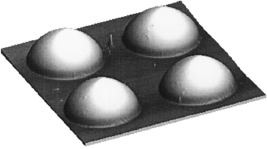
GaN micro-light-emitting diode arrays with monolithically integrated sapphire microlenses
– HW Choi, C Liu, E Gu, G McConnell, JM Girkin, IM Watson, and MD Dawson
Applied Physics Letters, vol. 84, 13, pp. 2253 (2004)
GaN micro-light-emitting diodes (micro-LEDs) with monolithically integrated microlenses have been demonstrated. Microlenses, with a focal length of 44 μm and a root mean square roughness of ∼1 nm, have been fabricated on the polished back surface of a sapphire substrate of an array of micro-LEDs by resist thermal reflow and plasma etching. The optical properties of the microlenses have been demonstrated to alter the emission pattern of the LED emitters. The cone of light emitted from this hybrid device is significantly less divergent than a conventional broad-area device. This combination of micro-LED and microlens technologies offers the potential for further improvement in the overall efficiency of GaN-based light emitters.
DOI: 10.1063/1.1690876
InGaN microring light-emitting diodes
– HW Choi, CW Jeon, and MD Dawson
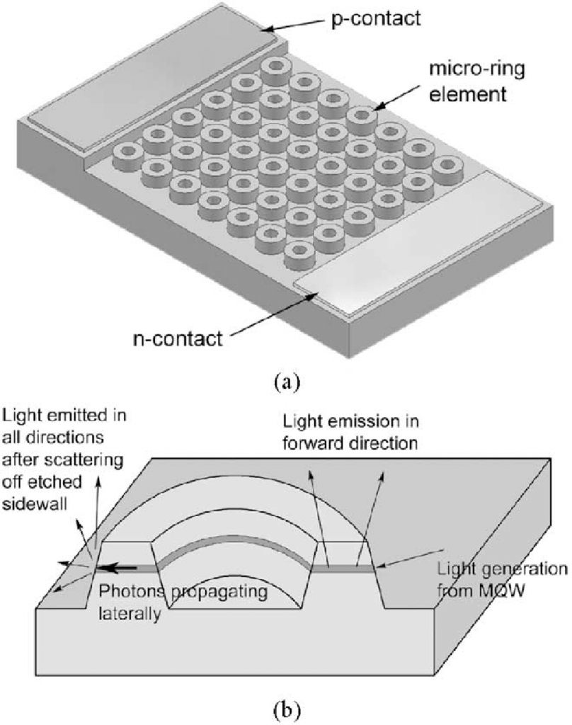
IEEE Photonics Technology Letters, vol. 16, 1, pp. 33-35 (2004)
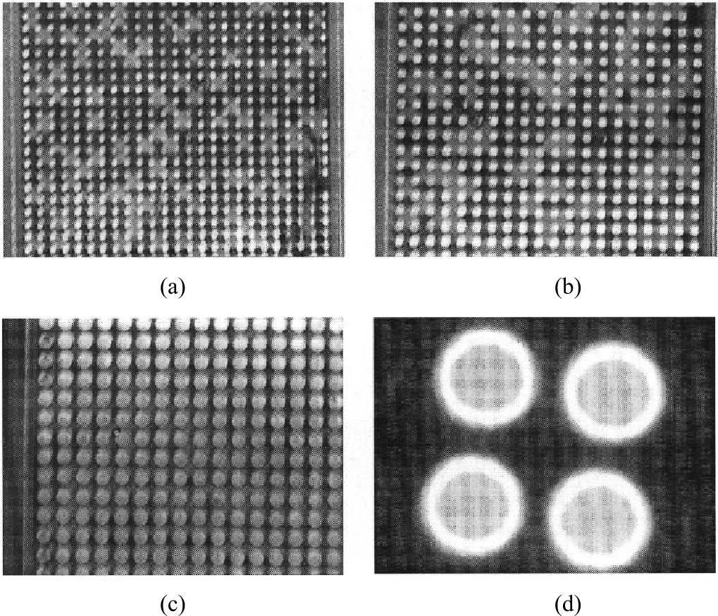
The fabrication and performance of an InGaN light-emitting diode (LED) array based on a microring device geometry is reported. This design has been adopted in order to increase the surface area for light extraction and to minimize losses due to internal reflections and reabsorption. Electrical characteristics of these devices are similar to those of a conventional large-area LED, while the directed light extraction proves to be superior. In fact, these devices are found to be more efficient when operated at higher currents. This may be attributed to improved heat sinking due to the large surface area to volume ratio. The potential applications of these devices are also discussed.
Fabrication and performance of parallel-addressed InGaN micro-LED arrays
– H.W. Choi, C.W. Jeon, M.D. Dawson, P.R. Edwards, and R.W. Martin
IEEE Photonics Technology Letters, vol. 15, 4, pp. 510-512 (2003).
High-performance, two-dimensional arrays of parallel-addressed InGaN blue micro-light-emitting diodes (LEDs) with individual element diameters of 8, 12, and 20 μm, respectively, and overall dimensions 490 ×490 μm, have been fabricated. In order to overcome the difficulty of interconnecting multiple device elements with sufficient step-height coverage for contact metallization, a novel scheme involving the etching of sloped-sidewalls has been developed. The devices have current-voltage (I-V) characteristics approaching those of broad-area reference LEDs fabricated from the same wafer, and give comparable (3-mW) light output in the forward direction to the reference LEDs, despite much lower active area. The external efficiencies of the micro-LED arrays improve as the dimensions of the individual elements are scaled down. This is attributed to scattering at the etched sidewalls of in-plane propagating photons into the forward direction.