Colourful chip-scale microLED displays
– HW Choi, WY Fu, and H Lyu
Compound Semiconductor, vol. 25, 5, pp. 18 (2019)
Patterning epiwafers with indium-rich InGaN quantum wells enables the fabrication of monolithic, full-colour displays
Read at Compound Semiconductor
Making monolithic integrated systems with GaN
– HW Choi, WY Fu, KH Li and YF Cheung

Compound Semiconductor, vol. 24, 2, pp. 54-57 (2018)
GaN produces great LEDs, lasers and transistors. Just imagine the possibilities when two or more of these classes of devices are united on the same chip.
Read at Compound Semiconductor
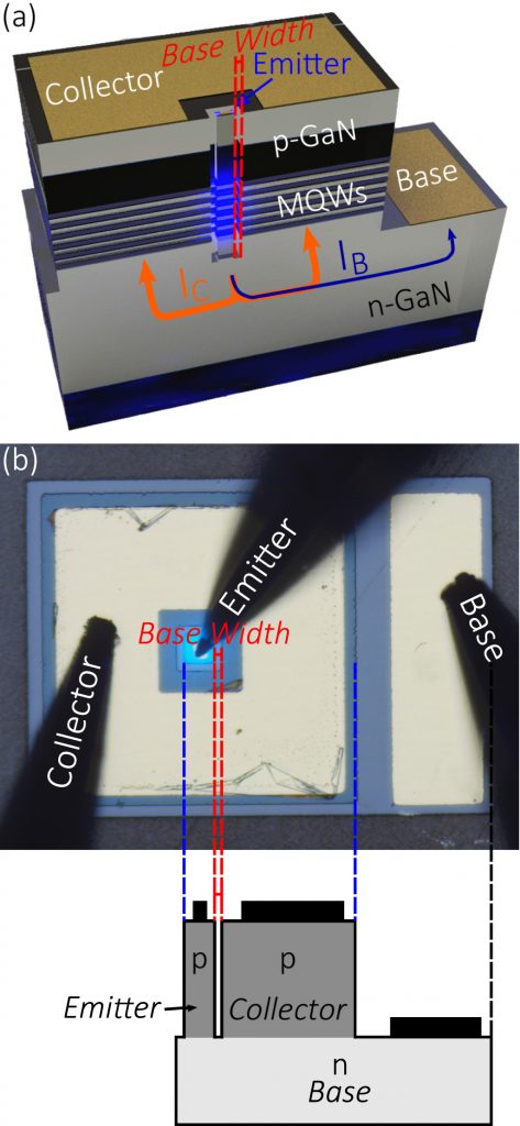
GaN PNP light-emitting bipolar junction transistor
– WY Fu, and HW Choi
Journal of Physics D: Applied Physics, vol. 55, 1, pp. 015101 (2021)
An light-emitting bipolar transistor (LEBJT) has been developed in response to aspirations for on-chip electronics with GaN-based light-emitting diode (LED) devices. The design utilizes the existing p-n junction of an LED structure to construct a PNP bipolar junction transistor comprising two back-to-back p-n junctions, saving the need for customized structures or epitaxial regrowth. Two designs of monolithic GaN LEBJTs have been demonstrated in this work—an LEBJT with a larger emitter area size for conversion of electronic to optical signal, as well as an LEBJT with reduced emitter area for boosting of current gain. Employing an emitter comprising an array of nanopillars patterned by nanosphere lithography, the LEBJT exhibits an average current gain of 20 and a bandwidth of 180 MHz.
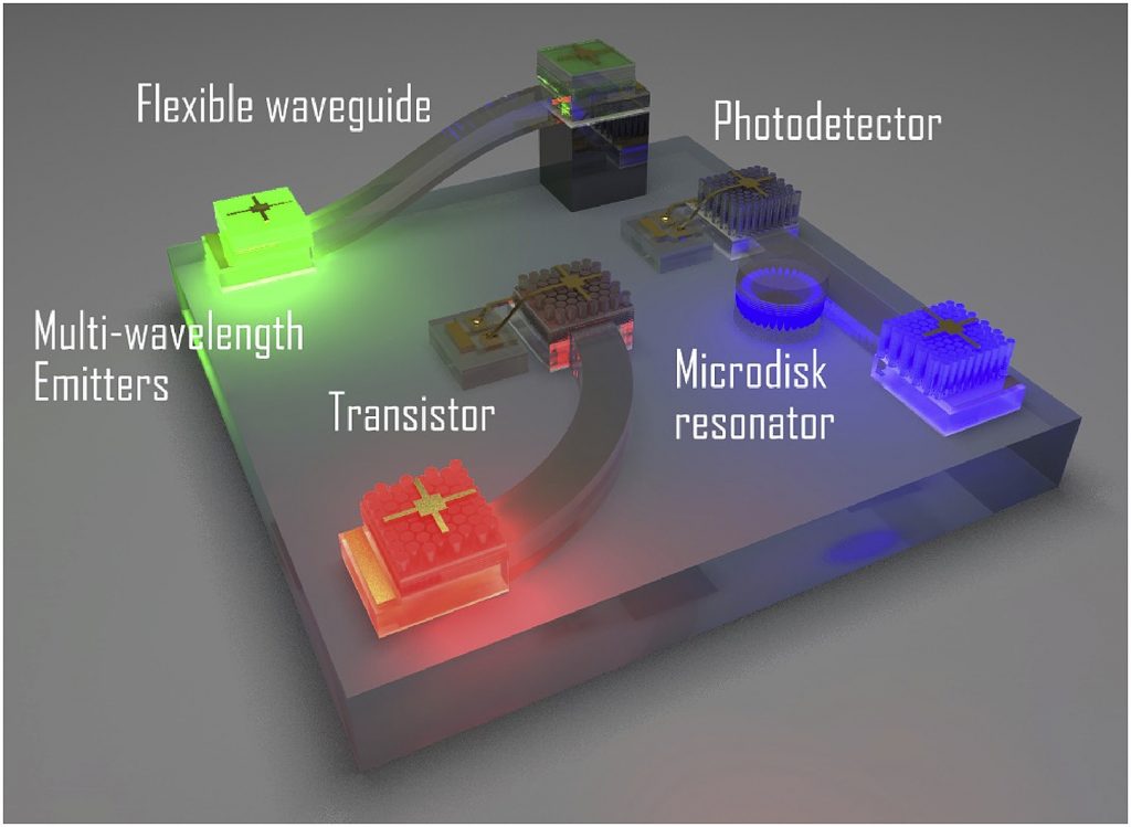
Chip-scale GaN integration
– KH Li, WY Fu, and HW Choi
Progress in Quantum Electronics, vol. 70, pp. 100247 (2020)
Blue LEDs and HEMTs based on III-Nitride have been flourishing commercially across the globe, thanks largely to breakthroughs in the material quality of the wide-bandgap compound semiconductor back in the 1990s. The realizations of white-light LEDs, blu-ray systems, and lately efficient compact chargers have drastically changed the way we live and have contributed tremendously to global energy saving efforts. The maturity and diversity of modern discrete GaN-based devices open up opportunities for an integrated GaN platform with extended functionalities and applications. In this review paper, we present an overview of the monolithic and heterogeneous integration of GaN devices and components. Various methods for the integration of electronic, optoelectronic, and optical components based on GaN are discussed.
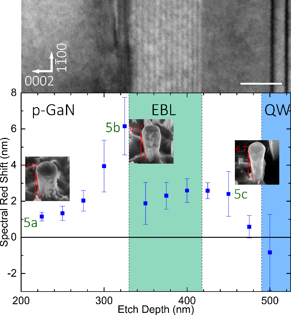
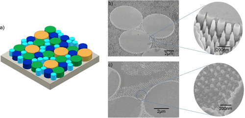
Strain-Induced Spectral Red-Shifting from Nanoscale Frustum Arrays Fabricated over InGaN/GaN Quantum Wells for Light-Emitting Applications
– WY Fu, and HW Choi
ACS Applied Nano Materials, vol. 4, 1, pp. 666-672 (2021)
While spectral blue-shifting caused by nanostructuring of InGaN/GaN quantum wells has been widely reported for altering the emission color of light-emitting diodes, the same cannot be said for spectral red-shifting. It is well-known that nanostructuring of the quantum wells gives rise to relaxation of the strain incurred in the quantum wells, reducing the quantum confined stark effect with a consequence of spectral shifting to shorter wavelengths. In this report, we demonstrate a nanostructure configuration that produces the opposite effect, spectral red-shifting, by increasing the strain in the quantum wells through the formation of an inverted nanoconical-frustum array over the quantum wells, without allowing the nanostructures to penetrate through the quantum wells. Under such conditions, spectral red-shifting of the photoluminescence spectrum can be observed, consistent with the prediction of strain induction in the quantum wells by molecular dynamics simulations. Experimentally, spectral red-shift of the photoluminescence spectrum by up to 7.6 nm has been observed, when the proposed nanostructures are fabricated on InGaN/GaN quantum wells grown on a c-plane sapphire substrate with a nominal emission wavelength of ∼560 nm.
InGaN RGB Light-Emitting Diodes With Monolithically Integrated Photodetectors for Stabilizing Color Chromaticity
– KH Li, YF Cheung, W Jin, WY Fu, ATL Lee, SC Tan, SY Hui, and HW Choi
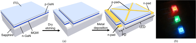
IEEE Transactions on Industrial Electronics, vol. 67, 6, pp. 5154-5160 (2020)
In this paper, a solution toward realizing color chromaticity stabilized InGaN red, green, and blue (RGB) light-emitting diode (LED) is proposed and demonstrated. The InGaN/GaN multiple quantum wells (play a key role in light emission from the LEDs and photodetection from the photodetectors (PDs). The spectral overlaps between the emission and absorption spectra are measured and the photocurrents of the PDs exhibit linear behavior with increasing LED driving currents. The solution involves the use of RGB chips with monolithically integrated PDs that detect the levels of light output from an individual chip in real time, whose photocurrent signals are fed to LED driver circuits that make use of the signal to provide a driving current that stabilizes the light output. Adoption of this feedback strategy results in CIE coordinates drifts of Δ(0.003, 0.005) over the 400 h duration of testing, proving to be an effective way of stabilizing color chromaticity from RGB LEDs.
Intensity-Stabilized LEDs With Monolithically Integrated Photodetectors
– KH Li, H Lu, WY Fu, YF Cheung, and HW Choi
IEEE Transactions on Industrial Electronics, vol. 66, 9, pp. 7426-7432 (2019)
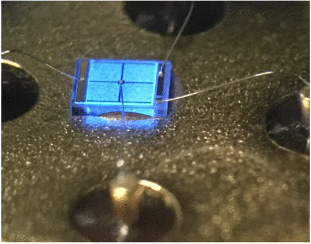
To overcome light output degradations and fluctuations of intensities from light-emitting diodes (LEDs) over time, the monolithic integration of InGaN LEDs and photodetectors (PDs) is demonstrated in this paper. The InGaN/GaN multiquantum wells (MQWs) play the role of light emission and detection from the LED and PD, respectively. Despite the larger bandgap energies of the InGaN layers, the MQWs absorb light emitted by the LED due to the band tail effect, extending the absorption range up to 460 nm, which correspond to the peak wavelength of emission. The tiny-sized PD detects light from the adjacent LED coupled through the sapphire substrate to generate a photocurrent that is proportional to its light output, but remains unresponsive to ambient lighting. Apart from real-time light output monitoring, the photocurrent can be used as a feedback signal for regulation of light output. A microcontroller-based feedback circuit has been implemented to drive the LED and the photocurrent level is maintained to a preset value by adjustment of the driving current. Using this scheme, light output from the LED is stabilized to within ~0.2% over 1-h periods.
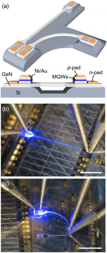
Monolithically integrated InGaN/GaN light-emitting diodes, photodetectors, and waveguides on Si substrate
– KH Li, WY Fu, YF Cheung, KKY Wong, Y Wang, KM Lau, and HW Choi
Optica, vol. 5, 5, pp. 564-569 (2018)
The characteristics of monolithically integrated light-emitting diodes (LEDs), photodetectors (PDs), and waveguides on a GaN-on-Si wafer are investigated. The InGaN/GaN multi-quantum wells, which are responsible for blue light emission in LEDs, are also used for photodetection in PDs. Despite the Stokes shift, a spectral overlap of ∼25 nm between the emission and absorption spectra provides the PDs with sufficient photosensitivity to signals from the emitter while remaining insensitive to ambient lighting. Optical interconnects in the form of linear or bent suspended waveguides bridging the LEDs and PDs are formed by selective detachment of etched GaN mesas from the Si substrate. Additionally, the PDs can be detached from the substrate and remounted on an elevated platform, owing to the flexibility of the thin-film waveguide. The 150 μm×150 μm LEDs and PDs exhibit rapid response on nanosecond time scales, which is attributed to fast radiative recombinations as well as minimized resistive-capacitive (RC) delays, enabling transmission of pseudorandom binary sequence (PRBS) data signals at rates of 250 Mb/s with an opening in the eye diagram. Together with multichannel transmission free of crosstalk, the ability of the planar and three-dimensional monolithic photonic systems to handle visible-light communication (VLC) applications is demonstrated.
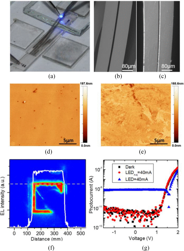
Monolithic Integration of GaN-on-Sapphire Light-Emitting Diodes, Photodetectors, and Waveguides
– KH Li, YF Cheung, WY Fu, KK Wong, and HW Choihoi
IEEE Journal of Selected Topics in Quantum Electronics, vol. 24, 6, pp. 1-6 (2018)
We demonstrate the monolithic integration of light-emitting diodes (LEDs), photodetectors (PDs), and waveguides on a GaN-on-sapphire wafer. The InGaN/GaN multi-quantum wells (MQWs) play a key role in light emission from the LED and photodetection from the PD. Despite large Stokes shift between absorption and emission energies in the InGaN layer, the MQWs are capable of absorbing light emitted by the LED due to the band tail effect, extending the absorption range up to 460 nm. The existence of optical crosstalk is mainly due to optical channeling in the transparent sapphire substrate beneath the LED, but can be eliminated by the detachment of the LED and waveguide via selective-area laser lift-off process. With the bendable waveguides and remounting of the LED onto an elevated platform, the feasibility of routing optical signal between two different planes is demonstrated. Apart from crosstalk-free performance, the three-dimensional system exhibits more than five times higher photocurrent than the planar system, attributed to spectral blue-shift of the LED and enhanced optical confinement in suspended waveguide. The LEDs and PDs also exhibit rapid response on the nanosecond time-scale, enabling transmission of data signals at rates of 250 Mb/s with an opening in the eye diagram.
Monolithic Broadband InGaN Light-Emitting Diode
– C Feng, J-A Huang, and HW Choi
ACS Photonics, vol. 3, 7, pp. 1294-1300 (2016)
A monolithic nonphosphor broadband-emission light-emitting diode is demonstrated, comprising a combination of high-density microstructured and nanostructured InGaN-GaN quantum wells fabricated using a top-down approach. Broadband emission is achieved by taking advantage of low-dimensional-induced strain-relaxation of highly strained quantum wells, combining light emitted from strain-relaxed nanotips at wavelengths shorter than the as-grown by as much as 80 nm with longer-wavelength light emitted from the larger nonrelaxed microdisks. The localized emission characteristics have been studied by spatially resolved near-field photoluminescence spectroscopy which enabled both the photoluminescence intensity and spectrum from individual nanotips to be distinguished from emission at the larger-dimensioned regions. Distinctive blue-green-yellow emission can be observed from the electroluminescent device, whose continuous broadband spectrum is characterized by CIE coordinates of (0.39, 0.47) and color rendering index of 41. Emission can be tuned by adjusting the relative densities of nanotips and microdisks along the linear color gamut defined by their respective CIE coordinates.
Confocal microscopic analysis of optical crosstalk in GaN micro-pixel light-emitting diodes
– KH Li, YF Cheung, WS Cheung, and HW Choi

Applied Physics Letters, vol. 107, 17, pp. 171103 (2015)
The optical crosstalk phenomenon in GaN micro-pixel light-emitting diodes (LED) has been investigated by confocal microscopy. Depth-resolved confocal emission images indicate light channeling along the GaN and sapphire layers as the source of crosstalk. Thin-film micro-pixel devices are proposed, whereby the light-trapping sapphire layers are removed by laser lift-off. Optical crosstalk is significantly reduced but not eliminated due to the remaining GaN layer. Another design involving micro-pixels which are completely isolated is further proposed; such devices exhibited low-noise and enhanced optical performances, which are important attributes for high-density micro-pixel LED applications including micro-displays and multi-channel optical communications.
DOI: 10.1063/1.4934840
III-nitride light-emitting diode with embedded photonic crystals
– KH Li, KY Zang, SJ Chua, and HW Choi
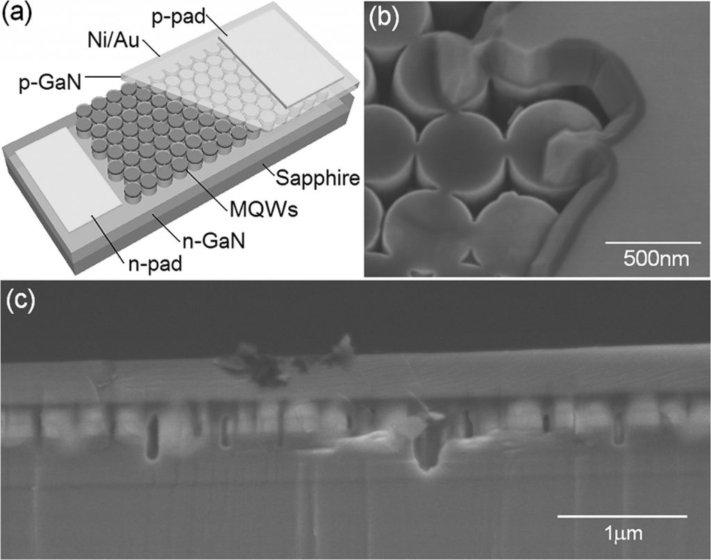
Applied Physics Letters, vol. 102, 18, pp. 181117 (2013)
A photonic crystal has been embedded within an InGaN/GaN light-emitting diode structure via epitaxial lateral overgrowth of a p-type GaN capping layer. The photonic crystal is a hexagonal-closed-packed array of nano-pillars patterned by nanosphere lithography; the capping layer planarizes the disconnected pillars to form a current-injection device. Optical properties of the nanostructures and devices are extensively studied through a range of spectroscopy techniques and simulations. Most significantly, the emission wavelengths of embedded photonic crystal light-emitting diodes are nearly invariant of injection currents, attributed to partial suppression of the built-in piezoelectric in the quantum wells.
DOI: 10.1063/1.4804678
Optical and Thermal Analyses of Thin-Film Hexagonal Micro-Mesh Light-Emitting Diodes
– KH Li, YF Cheung, Q Zhang, and HW Choi
IEEE Photonics Technology Letters, vol. 25, 4, pp. 374-377 (2013)
Vertical thin-film light-emitting diodes (LEDs) with integrated micro-mesh arrays are reported. By removing the sapphire substrate through laser lift-off, vertical current conduction becomes possible, improving current spreading capability and thus electrical properties. Compared with the as-grown device, the thin-film micro-mesh LEDs emits 61% more optical power, attributed to enhanced light extraction through the micro-mesh, evidence of which is provided by confocal imaging. At 100 mA, the enhancement factor rises to >;100% attributed to low junction temperatures due to efficient heat conduction as verified by infrared thermometric imaging.
The contribution of sidewall light extraction to efficiencies of polygonal light-emitting diodes shaped with laser micromachining
– XH Wang, PT Lai, and HW Choi
Journal of Applied Physics, vol. 108, 2, pp. 023110 (2010)
The light extraction efficiencies of InGaN/GaN blue light-emitting diodes (LEDs) of different geometries ranging from a triangle to a decagon have been simulated by ray-tracing. The conventional rectangular LED was found to be the most inefficient among the investigated polygons, and light extraction through the device sidewalls was the key factor. The results were experimentally verified by fabricating LEDs shaped into polygons by nanosecond-pulsed laser micromachining, which proved the simulated results. The mechanism of light extrac-tion in polygonal LEDs is discussed in detail.
Mechanism of optical degradation in microstructured InGaN light-emitting diodes
– ZL Li, KH Li, and HW Choi
Journal of Applied Physics, vol. 108, 11, pp. 114511 (2010)
While the enhancement of light extraction efficiency from microstructured InGaN light-emitting diodes (?LED) has been firmly established, there is concern over the effect of microstructuring on the device lifetimes. A study on the electrical characteristics and reliability of ?LED arrays has been carried out. Despite improved optical performance, expanded device sidewalls served to accelerate the rate of optical degradation, adversely affect the lifetimes of devices. Through current-voltage plots and noise spectrum measurements, vertical current conduction along the plasma-damaged sidewalls was identified as the key degradation mechanism.
DOI: 10.1063/1.3517829
Evaluation of InGaN/GaN light-emitting diodes of circular geometry
– XH Wang, WY Fu, PT Lai, and HW Choi
Optics Express, vol. 17, 25, pp. 22311-22319 (2009)
Blue GaN light emitting diodes (LEDs) in the shape of cuboids and circular disks have been fabricated by laser micromachining. The proposed circular geometry serves to enhance overall light extraction on a macro-scale and to improve uniformity of the emission pattern due to the rotational symmetry of the chip. Analysis of the chip shaping effect is carried out by ray-tracing simulations and further supported with mathematical modeling using ideal LED models, and subsequently verified with fabricated devices. In comparison, a 10% improvement in overall emission was observed for circular LEDs over the regular cuboids, consistent with simulations and calculations. The measured emission pattern from the circular LED confirms the axial symmetry of the emission beam.
DOI: 10.1364/OE.17.022311
Geometrical Shaping of InGaN Light-Emitting Diodes by Laser Micromachining
– WY Fu, KN Hui, XH Wang, KKY Wong, PT Lai, and HW Choi
IEEE Photonics Technology Letters, vol. 21, 15, pp. 1078-1080 (2009)
Geometrical shaping of InGaN light-emitting diodes (LEDs) by laser micromachining is introduced. The sapphire substrate is shaped with inclined sidewalls at 50deg, serving as a prism favoring light redirection for out-coupling from the top window. Compared to conventional cuboid LEDs with a calculated light extraction efficiency eta ext of 18.3%, these shaped LEDs offers a pronounced increase in eta ext of up to 85.2%, verified by experimental results.
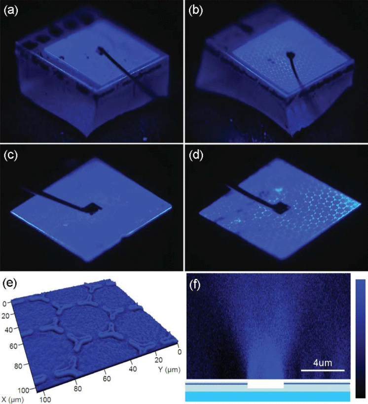
Photonic crystal light-emitting diodes fabricated by microsphere lithography
– WN Ng, CH Leung, PT Lai, and HW Choi
PhC LED (bottom) driven at 1.5 mA.
Nanotechnology, vol. 19, 25, pp. 255302 (2008)
Instead of using conventional electron lithography, a two-dimensional photonic crystal consisting of a hexagonal array of triangular air-holes was created on the surface of a GaN LED substrate using microsphere lithography. The microspheres self-assemble into a single-layered hexagonal-close-packed array acting as an etch mask. A significant enhancement in photoluminescence intensity was recorded from the PhC LED structure. A twofold increase in electroluminescence was observed from the PhC LED compared to an as-grown LED with identical geometry. Besides geometrical factors due to surface roughening, the dispersive nature of PhCs and diffractive properties of the PhC as a grating contribute to the enhancement of light extraction from the LED.
InGaN nano-ring structures for high-efficiency light emitting diodes
– HW Choi, CW Jeon, C Liu, IM Watson, MD Dawson, PR Edwards, RW Martin, S Tripathy, and SJ Chua
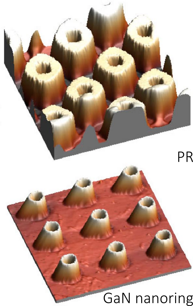
Journal of Crystal Growth, vol. 268, 3-4, pp. 527-530 (2004)
A novel method of etching which allows the direct interconnection of multiple GaN-based devices is introduced. The mesa structures of devices are etched using an isotropic recipe which produces tapered sidewalls. The extent of inclination can be readily controlled through variA technique based on the Fresnel diffraction effect for the fabrication of nano-scale site-controlled ring structures in InGaN/GaN multi-quantum well structures has been demonstrated. The ring structures have an internal diameter of 500 nm and a wall width of 300 nm. A 1cm−1 Raman shift has been measured, signifying substantial strain relaxation from the fabricated structure. The 9 nm blueshift observed in the cathodoluminescence spectra can be attributed to band filling and/or screening of the piezoelectric field. A light emitting diode based on this geometry has been demonstrated.
DOI: 10.1063/1.1849439
Fabrication of matrix-addressable micro-LED arrays based on a novel etch technique
– HW Choi, CW Jeon, and MD Dawson
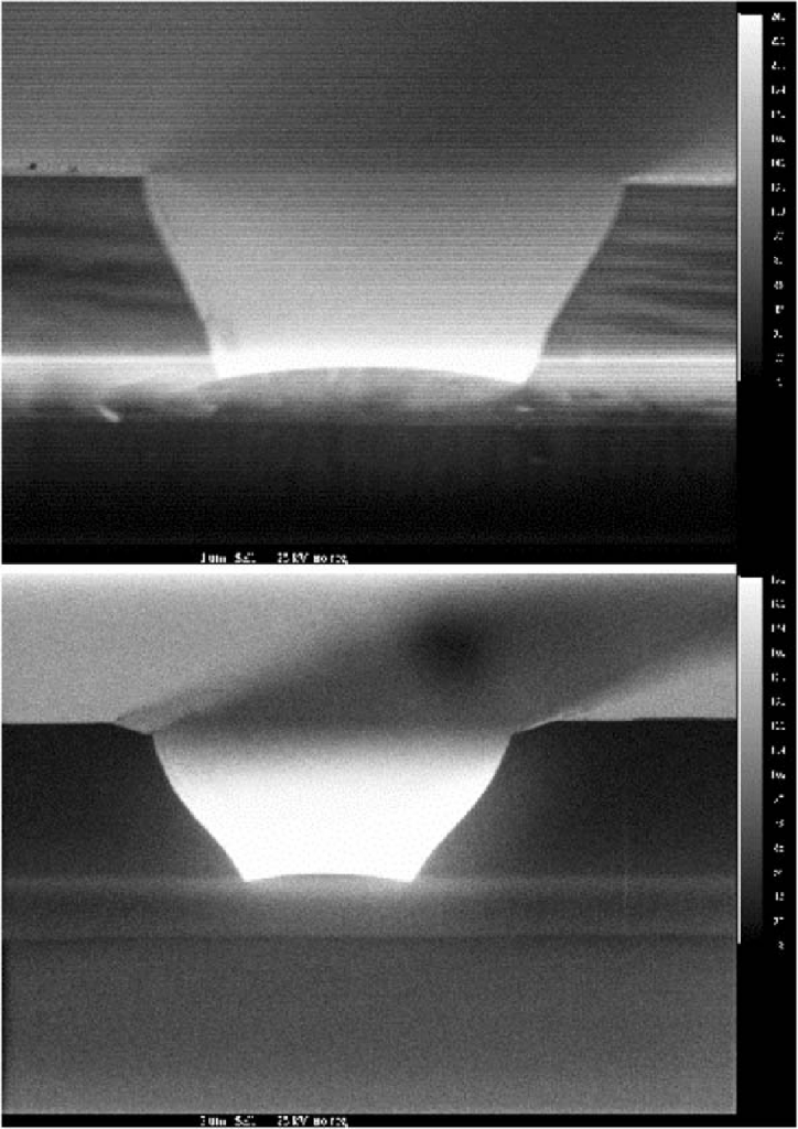
Journal of Crystal Growth, vol. 268, 3-4, pp. 527-530 (2004)
A novel method of etching which allows the direct interconnection of multiple GaN-based devices is introduced. The mesa structures of devices are etched using an isotropic recipe which produces tapered sidewalls. The extent of inclination can be readily controlled through various etching parameters, which include the ICP power, plate power and pressure, thus modifying the vertical and lateral etch components. This approach has been successfully adopted in the fabrication of interconnect and matrix-addressable micro-LEDs, which offer superior optical and electrical performance and a high degree of uniformity compared to similar devices fabricated using conventional processes.
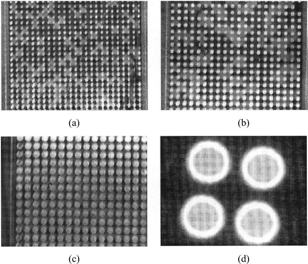
High-resolution 128 x 96 nitride microdisplay
– HW Choi, C Liu, E Gu, G McConnell, JM Girkin, IM Watson, and MD Dawson
IEEE Electron Device Letters, vol. 25, 5, pp. 277-279 (2004)
Matrix-addressable arrays of InGaN micro-light-emitting diodes with 128 × 96 pixels and a resolution of 1200 dpi have been fabricated using a novel “sloped sidewall” process. The devices have been fabricated on InGaN blue and green wafers, emitting light at the wavelengths of 468 and 508 nm, respectively. A simple circuit, which enables the display of an arrow pattern with ~60% of the pixels turned on, was used for device testing. At an injection current of 60 mA, the devices deliver 3.3 (blue) and 2.4 mW (green) of output power, corresponding to a luminance of more than 30 000 Cd/m2. These high-brightness and highly versatile devices are certainly an attractive form of emissive micro-display.
GaN micro-light-emitting diode arrays with monolithically integrated sapphire microlenses
– HW Choi, C Liu, E Gu, G McConnell, JM Girkin, IM Watson, and MD Dawson
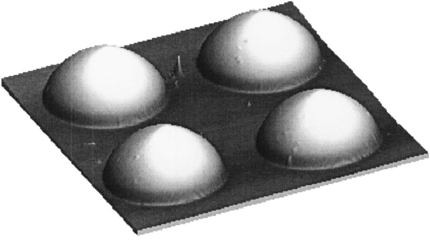
Applied Physics Letters, vol. 84, 13, pp. 2253 (2004)
GaN micro-light-emitting diodes (micro-LEDs) with monolithically integrated microlenses have been demonstrated. Microlenses, with a focal length of 44 μm and a root mean square roughness of ∼1 nm, have been fabricated on the polished back surface of a sapphire substrate of an array of micro-LEDs by resist thermal reflow and plasma etching. The optical properties of the microlenses have been demonstrated to alter the emission pattern of the LED emitters. The cone of light emitted from this hybrid device is significantly less divergent than a conventional broad-area device. This combination of micro-LED and microlens technologies offers the potential for further improvement in the overall efficiency of GaN-based light emitters.
DOI: 10.1063/1.1690876
InGaN microring light-emitting diodes
– HW Choi, CW Jeon, and MD Dawson
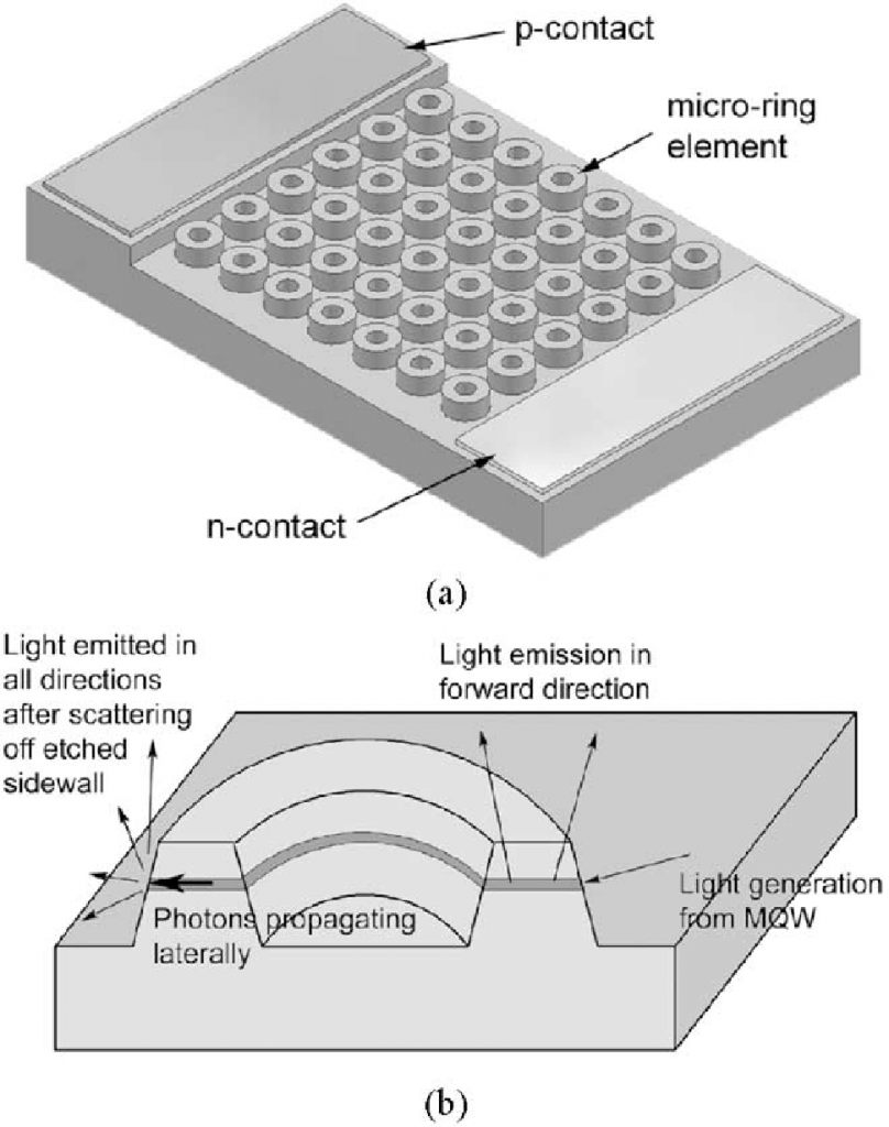
IEEE Photonics Technology Letters, vol. 16, 1, pp. 33-35 (2004)
The fabrication and performance of an InGaN light-emitting diode (LED) array based on a microring device geometry is reported. This design has been adopted in order to increase the surface area for light extraction and to minimize losses due to internal reflections and reabsorption. Electrical characteristics of these devices are similar to those of a conventional large-area LED, while the directed light extraction proves to be superior. In fact, these devices are found to be more efficient when operated at higher currents. This may be attributed to improved heat sinking due to the large surface area to volume ratio. The potential applications of these devices are also discussed.
Mechanism of enhanced light output efficiency in InGaN-based microlight emitting diodes
– HW Choi, CW Jeon, MD Dawson, PR Edwards, RW Martin, and S Tripathy
Journal of Applied Physics, vol. 93, 10, pp. 5978 (2003)
Micro-light emitting diode (LED) arrays with diameters of 4 to 20 μm have been fabricated and were found to be much more efficient light emitters compared to their broad-area counterparts, with up to five times enhancement in optical power densities. The possible mechanisms responsible for the improvement in performance were investigated. Strain relaxation in the microstructures as measured by Raman spectroscopy was not observed, arguing against theories of an increase in internal quantum efficiency due to a reduction of the piezoelectric field put forward by other groups. Optical microscope images show intense light emission at the periphery of the devices, as a result of light scattering off the etched sidewalls. This increases the extraction efficiency relative to broad area devices and boosts the forward optical output. In addition, spectra of the forward emitted light reveal the presence of resonant cavity modes [whispering gallery (WG) modes in particular] which appear to play a role in enhancing the optical output.
DOI: 10.1063/1.1567803
Fabrication and performance of parallel-addressed InGaN micro-LED arrays
– H.W. Choi, C.W. Jeon, M.D. Dawson, P.R. Edwards, and R.W. Martin
IEEE Photonics Technology Letters, vol. 15, 4, pp. 510-512 (2003).
High-performance, two-dimensional arrays of parallel-addressed InGaN blue micro-light-emitting diodes (LEDs) with individual element diameters of 8, 12, and 20 μm, respectively, and overall dimensions 490 ×490 μm, have been fabricated. In order to overcome the difficulty of interconnecting multiple device elements with sufficient step-height coverage for contact metallization, a novel scheme involving the etching of sloped-sidewalls has been developed. The devices have current-voltage (I-V) characteristics approaching those of broad-area reference LEDs fabricated from the same wafer, and give comparable (3-mW) light output in the forward direction to the reference LEDs, despite much lower active area. The external efficiencies of the micro-LED arrays improve as the dimensions of the individual elements are scaled down. This is attributed to scattering at the etched sidewalls of in-plane propagating photons into the forward direction.